
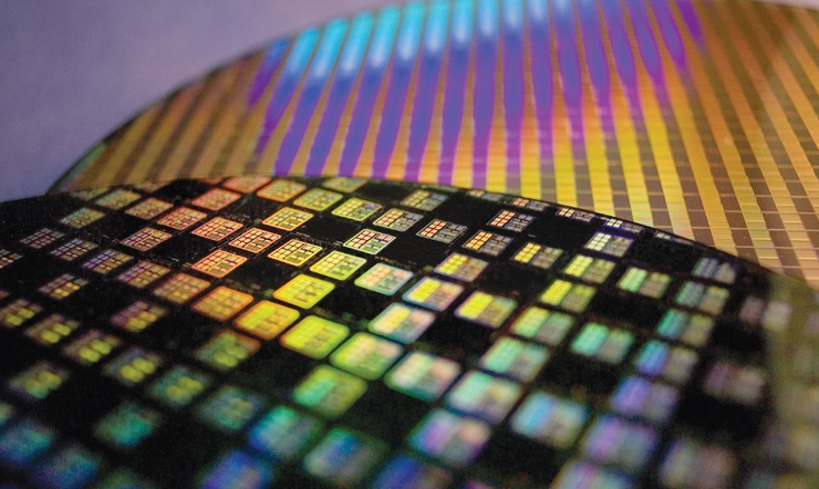
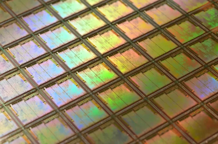
Patterned silicon wafers are an essential part of the semiconductor industry and have a variety of applications and advantages. They are crucial in the modern digital age, from computer chips and solar cells to nanotechnology and biomedical sensors.
Their role ranges from simple resistors and transistors to highly complex logic circuits and integrated systems. While the basic use of these wafers as raw materials is vital in modern technology, patterned wafers offer even greater possibilities for engineering applications. In this article, we’ll look at the different types of patterned silicon wafers, their use in various applications, and their advantages. With the right information, we can better understand the importance of patterned silicon wafers and their many possibilities.
Why Are Patterned Silicon Wafers Important In Today’s World?
The importance of these future technologies lies in their ability to enable manufacturers to produce smaller chips at higher speeds than ever before – something known as Moore’s Law. As technology advances, so does our need for faster processors; this means more efficient use of space within a chip package by packing more features into less area while still maintaining performance levels required by today’s applications.
What Are Patterned Silicon Wafers?

They are thin discs of semiconductor material used to manufacture integrated circuits. The patterned nature refers to the detailed photo-lithographic process used to create various layers on their surface and form specific components, such as transistors or resistors.
Patterning involves coating a base layer – typically of oxidized or doped silicon – with a photoresist, exposing it to light via an image mask, and finally etching away all exposed areas. This process is repeated several times until each layer has been etched according to its design specifications. As this procedure requires high precision and expertise, many companies outsource their patterning needs rather than attempt it in-house.
How Are They Made?
They are made through a process called photolithography. This involves creating patterns on the wafer surface by transferring patterns onto the wafer with light. This process is usually done in a clean room environment to prevent dust and other particles from contaminating the wafer.
It all starts with the raw material: a polished silicon wafer, which is basically a thin slice cut from polycrystalline or monocrystalline ingots of pure silicon. This disc then passes through several steps to make it ready for patterning.
First, the wafer is coated with a photosensitive material. It is applied to protect any areas that need to stay unaffected during etching – think of it like pre-marking where notches can go and which parts will remain untouched when exposed to certain materials. The photoresist can be either positive or negative, depending on the type of photolithography process used.
Now the pattern is transferred onto the wafer using an ultraviolet (UV) light source. Sometimes, a special mask may block certain portions of the wafer from the UV light. When the UV light reaches the exposed portions of the wafer, it causes a chemical reaction in the photosensitive material that creates a pattern.
Once the pattern has been created, any remaining photosensitive material must be removed from the wafer. This is followed by using a special chemical solvent or heat. When it is complete it is possible to print hundreds or even thousands or millions of detailed features on each square millimeter of the wafer.
What Are Their Applications?

Patterned Silicon Wafers have become an increasingly popular technology due to their many advantages over traditional silicon wafers. These advanced wafers can be used in various applications, from consumer electronics to industrial manufacturing. Here is a look at some of the most common uses for patterned silicon wafers:
- Microelectronics: It can be used to create transistors, capacitors, resistors, and other components like microprocessors and integrated circuits (ICs).
- Photovoltaics: These wafers can also be used as solar cells in photovoltaic systems such as those found on satellites or spacecraft.
- Medical Devices: Patterned silicon wafers have been instrumental in creating smaller medical devices like pacemakers or hearing aids, which require precise control over electrical signals within their circuitry.
- Automotive Components: As cars become increasingly automated, they rely heavily on sophisticated sensors and chipsets made using patterned silicon technology. From driverless car navigation systems to advanced safety features such as lane departure warnings, these components play an integral role in automotive engineering today.
- Sensors: Patterned silicon wafer technology has enabled sensors with higher sensitivity than ever possible due to its ability to precisely measure changes in voltage across different points on the chip surface. This makes them ideal for measuring temperature, pressure, humidity, etc.
Advantages Of Using Patterned Silicon Wafers
Patterned Silicon Wafers have a variety of advantages that have helped revolutionize the semiconductor industry. These benefits include:
- Cost: Manufacturers use a patterning technique like photolithography by eliminating unnecessary steps or materials in the process that help to reduce the cost associated with the production of wafers.
- Reliability: The patterns of the surface create uniformity across each chip which leads to increased reliability for testing and use in different products. It also has the ability to create highly complex structures without compromising structural integrity or electrical properties.
- Performance: The etching process creates tiny channels on the surface which allow for better heat dissipation. And due to its precision, it improves device performance which makes it ideal for applications such as microprocessors, radio frequency transceivers, and digital signal processors.
- Flexibility: With patterning technologies, engineers have much more flexibility when designing new components or devices. They can easily adjust parameters such as feature size, line widths, spacing between lines, etc., allowing them to quickly test different designs without going through an entire fabrication cycle each time.
Conclusion
Patterned Silicon Wafers has revolutionized many industries due to its ability to create intricate patterns at a microscopic scale while maintaining accuracy throughout the process. As this technology continues to evolve, it will open up new possibilities across multiple fields, including healthcare, aerospace engineering, robotics, artificial intelligence, consumer electronics, and much more.
By understanding the process of creating patterned silicon wafers and the applications and advantages they offer, companies and consumers can make informed decisions about their technology and materials. With improved performance, greater flexibility, and reduced costs, patterned silicon wafers are sure to play an essential role in the future of technology.